
BoardLab
Review the board before bring-up.
Upload a KiCad project or netlist + BOM. BoardLab reads the datasheets, grades rails and interfaces, and returns a report you can act on.
Three steps from files to report.
01
Create a project
Open BoardLab and start a new project. Prefer a KiCad folder that contains the .kicad_pro — BoardLab loads sheets and board from there.
02
Upload what you have
KiCad: the project folder (or a zip with .kicad_pro at the root). Other tools: PADS/EDIF netlist + BOM (CSV/XLSX) with designators and full MPNs.
03
Run analysis
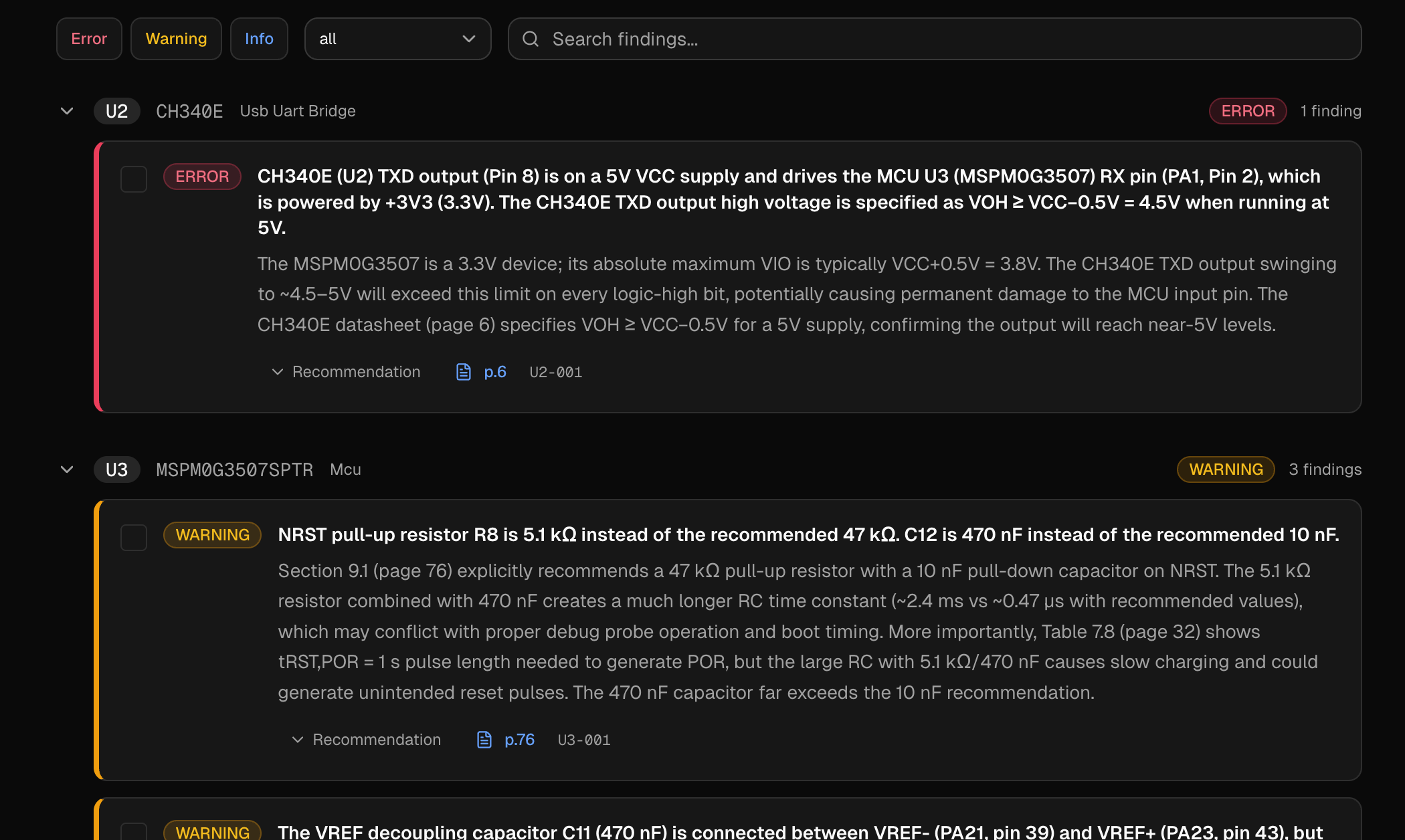
BoardLab reads datasheets, builds the design graph, grades rails and protocol interfaces, and writes a schema/PCB report you can share.
What BoardLab needs from you
Full instructions live under File upload guide. The short version:
- Manufacturer part numbers (orderable MPNs) — values alone are not enough
- Connectivity: KiCad project, or a PADS-PCB / EDIF netlist
- Optional .kicad_pcb beside the .kicad_pro for placement, pairs, and Z0
Ready when your schematic is.
Questions? mikbigi@gmail.com